This is a tutorial I wrote for the "Digital Systems Design" course as an introduction to sequential design. "4-bit Serial Adder/Subtractor with Parallel Load" is a simple project which may help to understand use of variables in the "process" statement in VHDL. However, basic understanding of the circuits is necessary, so both schematics and VHDL implementations are given. All code is written for Basys2 development board and Xilinx ISE was used as a synthesizer/simulator.
The Circuit
A 4-bit serial adder circuit consists of two 4-bit shift registers with parallel load, a full adder, and a D-type flip-flop for storing carry-out. A simplified schematics of the circuit is shown below:
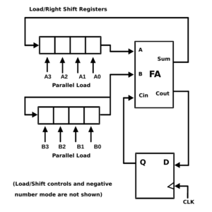
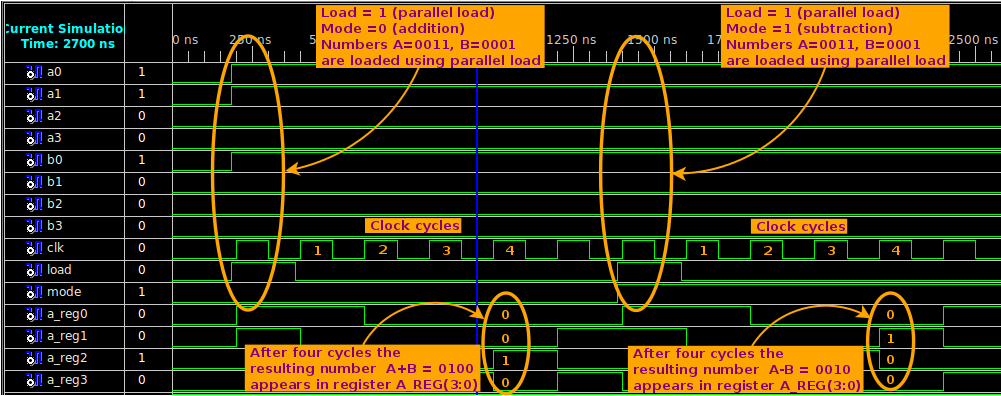
In order to load registers A_REG and B_REG with numbers, shift capability of the registers should be disabled and loading mode should be enabled. Loading of numbers from inputs A, B to registers A_REG, B_REG occurs in one clock cycle. After loading registers with numbers, shifting mode should be enabled to perform the arithmetic operation. The addition of numbers stored in A_REG and B_REG requires 4 cycles. Starting with the least significant bit, at each cycle one bit of number A and one bit of number B are being added. The sum is stored at the most significant bit of register A_REG. Carry-out output produced after each cycle is fed back to the full adder as a carry-in of the next significant bit. For this purpose one D-type flip-flop is used as a temporary storage element. The least significant bit of B_REG is fed to the input of the most significant bit of B_REG. Hence the circuit performs rotation operation for register B_REG.
Schematic Design in Xilinx ISE
Clone the project and checkout commit 5c385071530140074c8aa53dc40297b752ab0bd7:
|
1
2
3
|
git clone https://github.com/isabekov/FourBitSerialAdderSubtractor
cd FourBitSerialAdderSubtractor
git checkout 5c385071530140074c8aa53dc40297b752ab0bd7
|
Newer version of the code (commit 92c9460c533a0748104cbfb56988732b5c4095b8) contains 7-segment display and a bus, which groups individual bits of numbers A and B. The new version is not covered in this tutorial.
Create a new project with name "FourBitSerialAdderSubtractorSCH" and add exisiting source files from the archive provided:
- Schematics/FourBitSerialAdderSubtractor.sch
- Schematics/FullAdder.sch
- Schematics/Basys2.ucf
- Schematics/FourBitSerialAdderSubtractorSimulation.vhw
If you click on "FourBitSerialAdderSubtractor.sch" file in the top design, you will see the circuit of the 4-bit serial adder/subtractor with parallel load as shown below:
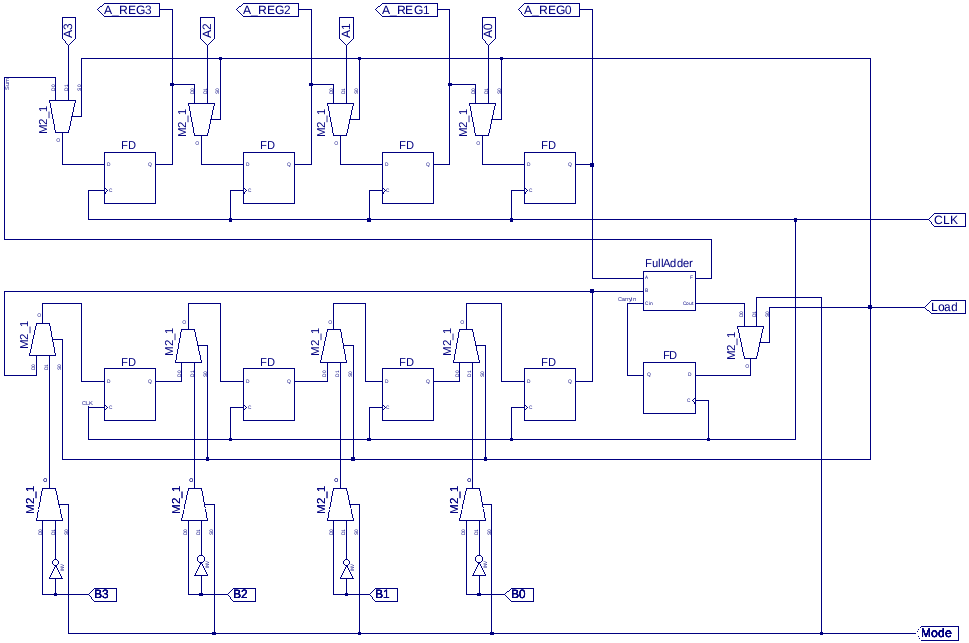
Number "B" can be negated in two’s complement form allowing subtraction operation mode. The symbols labeled with "M2_1" are 2-to-1 multiplexers. "FD"s are D-type flip-flops. Full adder circuit is used as a module "FullAdder.sch". Its schematics is given below:

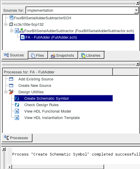
If you press on "Generate Programming File" under "Processes" panel, you will get an error:
|
1
|
Error : Symbol Not Found: FullAdder
|
In order to overcome this, you should create a symbol for the full adder module by going to "Sources" -> "Implementation" and choosing the "FA - FullAdder" line under "FourBitSerialAdderSubtractor" top design. After selecting it, expand "Design Utilities" section and press on "Create Schematic Symbol". The procedure is shown below:
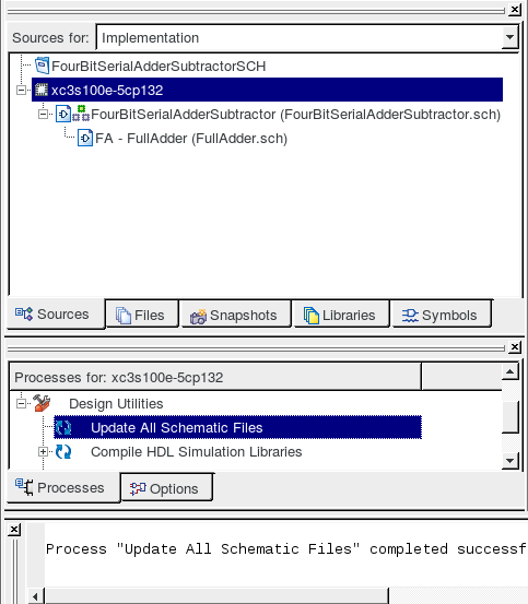
Now you have to update all schematic files. Go to device "Sources" -> "Implementation" and choose the "xc3s100e-5cp132" device. After selecting it, expand "Design Utilities" section and press on "Update All Schematic Files". The procedure is shown below:
The files are ready to use now. "FourBitSerialAdderSubtractorSimulation.vhw" is a VHDL file needed to simulate the circuit behavior. This simulates addition of two numbers: A=3 and B=1 and their subsequent subraction. You may also create a test bench waveform to simulate the circuit behavior instead. As explained in figure below the result of the arithmetical operation (addition/subtraction depending on the mode) will appear in register A_REG after 4 cycles:
Design Using VHDL
Clone the project:
|
1
2
|
git clone https://github.com/isabekov/FourBitSerialAdderSubtractor
cd FourBitSerialAdderSubtractor
|
Create a new project with name "FourBitSerialAdderSubtractorVHDL" and add exisiting source files from the downloaded directory:
- VHDL/FourBitSerialAdderSubtractor.vhd
- VHDL/FourBitSerialAdderSubtractorSimulation.vhw
- VHDL/Basys2.ucf
The code of the 4-bit serial adder/subtractor is given in "FourBitSerialAdderSubtractor.vhd". Sequential part requires using "process()" statement:
|
1
2
3
4
|
process(sensitivity list arguments)
begin
-- Process body
end process;
|
A process has a "sensitivity list" given as input arguments. Whenever the value of one of the signals in the sensitivity list changes, the process is executed. For example, "process(CLK)" means that whenever the clock signal "CLK" changes (it can be both rising and falling edge), the process is executed.
If-then-else statements can be used only within the process statements. Using if-then-else statements outside the process will yield an error. Positive-edge-triggered D-type flip-flop is implemented by checking the rising edge of the clock signal using if-then-else statement. A typical implementation of the D-type flip-flop is given below:
|
1
2
3
4
5
6
7
|
process(CLK)
begin
if(rising edge(CLK)) then
-- Flip-flop or register transfer operation
-- for example, X <= (A & B);
end if;
end process;
|
There is a big difference between a signal and a variable. A variable is defined in the beginning of the process and has an immediate behavior. The assignment of the value to the variable occurs immediately with no delay:
|
1
2
3
4
5
6
7
8
9
10
11
12
13
|
architecture Behavioral of Dummy is
-- Some intermediate signals
begin
process(CLK)
variable Sum: STD LOGIC; -- Sum is a variable
begin
if(rising edge(CLK)) then
Sum := (A_Reg(0) xor B_Reg(0)) xor (CarryOut);
-- The current (immediate) value of Sum is assigned to the MSB of A_Reg
A_Reg <= (Sum & A_Reg(3 downto 1));
end if;
end process;
end Behavioral;
|
Signal on the other hand can be considered as a flip-flop (or a register). The assignment of the value to the signal (i.e. signal transfer) occurs only after one clock cycle:
|
1
2
3
4
5
6
7
8
9
10
11
12
13
|
architecture Behavioral of Dummy is
-- Some intermediate signals
signal Sum: STD LOGIC; -- Sum is a signal
begin
process(CLK)
begin
if(rising edge(CLK)) then
Sum <= (A_Reg(0) xor B_Reg(0)) xor (CarryOut);
-- The previous (old) value of Sum is assigned to the MSB of A_Reg
A_Reg <= (Sum & A_Reg(3 downto 1));
end if;
end process;
end Behavioral;
|
This may be a reason for many bugs.
The code of the 4-bit serial adder/subtractor with parallel load is given below:
|
1
2
3
4
5
6
7
8
9
10
11
12
13
14
15
16
17
18
19
20
21
22
23
24
25
26
27
28
29
30
31
32
33
34
35
36
37
38
39
40
41
42
43
44
45
46
47
48
49
50
51
52
53
54
55
56
57
58
59
60
61
62
63
64
65
66
67
68
69
70
71
72
73
74
75
|
library IEEE;
use IEEE.STD_LOGIC_1164.ALL;
entity FourBitSerialAdderSubtractor is
generic (N : INTEGER:=4); -- N-bit Serial Adder/Subtractor
port(
A: in STD_LOGIC_VECTOR (N-1 downto 0); -- Input number A
B: in STD_LOGIC_VECTOR (N-1 downto 0); -- Input number B
CLK: in STD_LOGIC; -- Clock signal
Mode: in STD_LOGIC; -- Operating mode (addition/subtraction)
Load: in STD_LOGIC; -- Parallel load
A_Reg_Out: out STD_LOGIC_VECTOR(N-1 downto 0); -- Output of register A
B_Reg_Out: out STD_LOGIC_VECTOR(N-1 downto 0); -- Output of register B
Sev_Seg_Out: out STD_LOGIC_VECTOR(6 downto 0)); -- Seven segment output
end FourBitSerialAdderSubtractor;
architecture Behavioral of FourBitSerialAdderSubtractor is
signal CarryOut: STD_LOGIC; -- Carry-out signal
signal A_Reg: STD_LOGIC_VECTOR(N-1 downto 0):=(others => '0'); -- Register A
signal B_Reg: STD_LOGIC_VECTOR(N-1 downto 0):=(others => '0'); -- Register B
begin
-------------- Sequential part --------------
process(CLK)
variable Sum: STD_LOGIC;
begin
if(rising_edge(CLK)) then
if (Load = '1') then
A_Reg <= A;
if (Mode = '0') then
-- Addition
B_Reg <= B;
CarryOut <= '0';
else -- Subtraction (two's complement of B is loaded into B_Reg)
-- By setting carry in (carry-out(0)) as "1", and negating number B
-- the two's complement representation is obtained
B_Reg <= not(B);
CarryOut <= '1';
end if;
else
-- Rotate right register B_Reg
B_Reg <= (B_Reg(0) & B_Reg(N-1 downto 1));
-- Full-adder: summation output is assigned to variable "Sum" (immediate)
Sum := (A_Reg(0) xor B_Reg(0)) xor (CarryOut);
-- Write sum output of the full-adder to the MSB of the register A_Reg
A_Reg <= (Sum & A_Reg(N-1 downto 1));
-- Write carry out output of the full-adder to the flip-flop
CarryOut <= (((A_Reg(0) xor B_Reg(0)) and CarryOut)) or (A_Reg(0) and B_Reg(0));
end if;
end if;
end process;
-------------- Combinational part ----------------
A_Reg_Out <= A_Reg; -- Map A_REG to LEDs
B_Reg_Out <= B_Reg; -- Map B_REG to LEDs
-- Seven segment display for register A_Reg
Sev_Seg_Out <= "0000001" when A_Reg = "0000" else
"1001111" when A_Reg = "0001" else
"0010010" when A_Reg = "0010" else
"0000110" when A_Reg = "0011" else
"1001100" when A_Reg = "0100" else
"0100100" when A_Reg = "0101" else
"0100000" when A_Reg = "0110" else
"0001111" when A_Reg = "0111" else
"0000000" when A_Reg = "1000" else
"0000100" when A_Reg = "1001" else
"0001000" when A_Reg = "1010" else
"1100000" when A_Reg = "1011" else
"0110001" when A_Reg = "1100" else
"1000010" when A_Reg = "1101" else
"0110000" when A_Reg = "1110" else
"0111000" when A_Reg = "1111" else
"0000001";
end Behavioral;
|
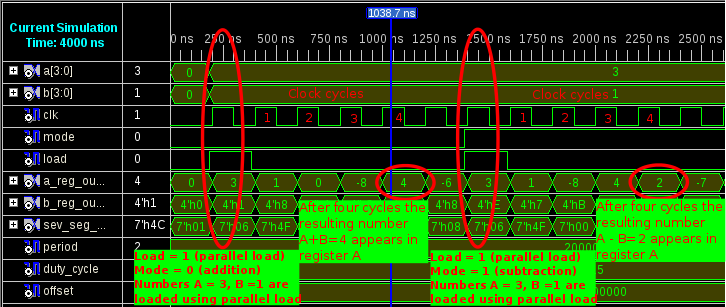
"Sum" and "CarryOut" are part of the full adder circuit. Number "B" is rotated in register B_Reg. Simulation using "FourBitSerialAdderSubtractorSimulation.vhw" file shows the same behavior as with the schematics version of the project:
After checking the pinouts of the circuit in the floorplan area or by editing the UCF-file which is given in "Basys2.ucf", the bit-file for flashing Basys2 board can be generated. Press on the "Generate Programming File" button. If the compilation process ends successfully, flash the Basys2 board with the generated bit-file using Adept program.
To test the circuit, firstly turn on and off proper switches which set numbers A and B. Then press on the "Load" button and keep holding. Click on the "CLK" button once. The numbers will be loaded into the registers. Release "Load" button and press on the "CLK" button 4 times. The result of the addition should appear on the LEDs. To perform subtraction, keep holding both "Mode" and "Load" buttons and click on the "CLK" button. Release all buttons and press on the "CLK" button 4 times. The result of the subtraction should appear on the LEDs. Note that the VHDL version of the circuit has a seven-segment display to show the content of register A_REG.
Demo: adding A and B, where A=2, B=3, the result 5 is shown after four clock cycles:
Demo: subtracting B from A, where A=4, B=1, the result 3 is shown after four clock cycles: